

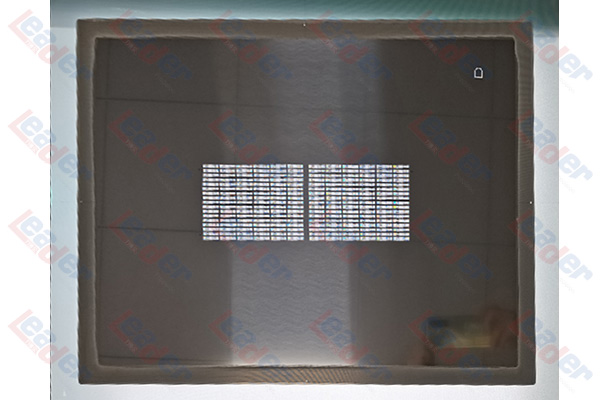
SIP, RF substrate electroforming printing template
The entity diagram is inconvenient to display, and this display diagram is a 3D rendering.
Uses: Used for system-level package printing flux and solder paste.
(Wearable equipment, manufactured by 5G wife elimination electronic package)
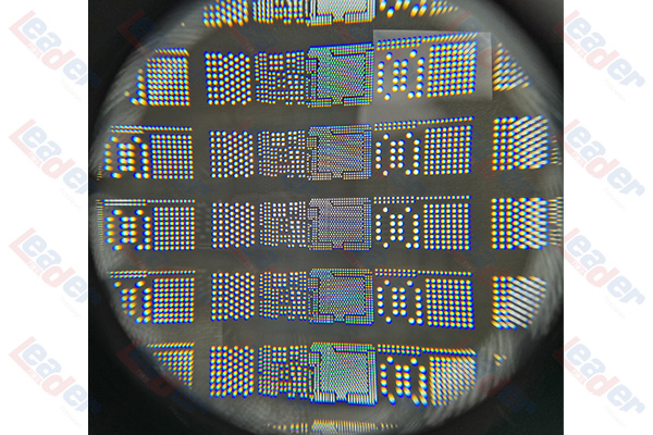
Main parameters:
Steel sheet thickness (t): 0.02 ~ 0.05 mm
Thickness error ±0.003mm;
The number of holes is 20,000 to 200,000.
The aperture is ≥0.05mm, and the opening accuracy is ±0.003mm
Opening position accuracy ±0.01mm
The solder paste template can make grooves on the non-printing surface to avoid Flux sticking.
Advantages: The electroforming process has high opening precision, smooth hole wall, good solder paste forming and good demoulding effect; And regardless of the number of holes, it is molded at one time.